
300mm Epitaxial Wafer
Wafer
SiC Wafer Targeting Sectors
The unique properties of silicon carbide (SiC) wafers and epitaxy offer the benefit of faster switching at higher power
and increased energy efficiency, often eliminating expensive cooling systems and enabling improved performance.
-

- Transportation
- Reduce the size and weight of
power modules while potentially increasing
a vehicle’s acceleration, range and/or speed,
with improved battery savings
(hybrid or electric vehicles, traction inverters
variable speed drives for electrical motor systems)
-

- Industrial
- New generation of industrial
motor controls and power supplies
(power factor correction and
uninterruptable power supplies)
-

- Energy
- Increase the efficiency and
performance of solar inverter and
wind turbine designs, as well as
providing the fundamental building
blocks for the emerging smart grid
(photovoltaic inverters)
SiC Wafer Portfolio
- 4H, 4° off-axis, n-type SiC wafers (substrates)
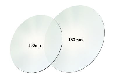
- Polished Wafer is a thin disc-shaped single crystal silicon carbide product manufactured from high-purity SiC crystals by physical vapor transport, which are subsequently sliced, polished and cleaned. It is produced in 100mm & 150mm diameters and are used in the manufacture of high power electronic devices such as Diodes, MOSFETs.
- SiC epitaxial wafer (n-type or p-type)
- Epitaxial Wafer is made by adding multi-micrometer thick single silicon carbide crystal layers on top of a polished wafer. Precise control of thickness, doping (carrier concentration) and defect density is required to enable high yielding power devices from a semiconductor fabrication facility. The range of epi products produced includes single-layer or multilayer n-type and p-type epitaxy.
ApplicationSchottky
Schottky Diode, Pin Diodes and Switches, High Current and Voltage MOSFETs / JFETs / BJTsPrime Grade Portfolio
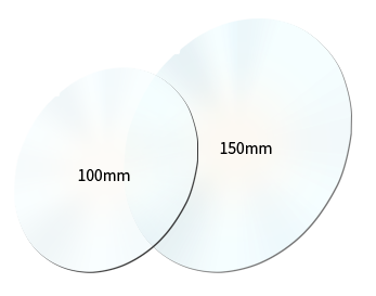
All SiC wafers in SK Siltron CSS’s 100 mm and 150 mm Prime Grade portfolios deliver consistently excellent mechanical
characteristics to ensure compatibility with existing and developing device fabrication processes.

- SiC wafers offer an attractive option for balancing performance and cost when designing simpler SiC power electronic components,such as Schottky or Junction Barrier Schottky diodes, with low to medium current ratings.
- - 100 mm : MPD (≤ 0.5 cm-2), EPD (≤ 12,000 cm-2), TED(≤ 9,000 cm-2), TSD (≤ 1,000 cm-2), BPD (≤ 2,000 cm-2)
- - 150 mm : MPD (≤ 1.0 cm-2), EPD (≤ 15,000 cm-2), TED(≤ 10,000 cm-2), TSD (≤ 3,000 cm-2), BPD (≤ 5,000 cm-2)

- SiC wafers deliver more stringent tolerances for defects, making them suitable for more demanding SiC devices like pin diodes or switches, and metal oxide semiconductor field effect transistors (MOSFETs).
- - 100 mm : MPD (≤ 0.2 cm-2), EPD (≤ 10,000 cm-2), TED(≤ 8,000 cm-2), TSD (≤ 800 cm-2), BPD (≤ 1,500 cm-2)
- - 150 mm : MPD (≤ 0.5 cm-2), EPD (≤ 12,000 cm-2), TED(≤ 9,000 cm-2), TSD (≤ 500 cm-2), BPD (≤ 4,000 cm-2)

- SiC wafers deliver the lowest defect densities and a tightened wafer resistivity distribution for the design of today's most advanced high-power SiC electronic devices, including MOSFETs junction field effect transistors (JFETs), and bipolar junction transistors (BJTs). In addition, the superior substrate quality can benefit high-voltage (3.3 kV and greater) and high-current device designs.
- - 100 mm : MPD (≤ 0.1 cm-2), EPD (≤ 8,000 cm-2), TED(≤ 6,000 cm-2), TSD (≤ 500 cm-2), BPD (≤ 1,000 cm-2)
- - 150 mm : MPD (≤ 0.3 cm-2), EPD (≤ 9,000 cm-2), TED(≤ 8,000 cm-2), TSD (≤ 400 cm-2), BPD (≤ 3,000 cm-2)