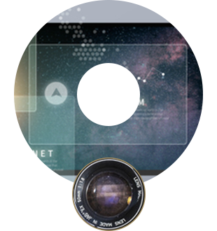
300mm Epitaxial Wafer
Wafer
Semiconductor Value Chain
-
 POLY SILICON
-
 INGOT / WAFER
-
 PATTERNED WAFER
-
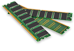
 SEMICONDUCTOR
-
 ELECTRNIC PRODUCT
200mm
300mm
- Polished Wafer
- Polished Wafer is a thin disc-shaped single crystal silicon product manufactured from high-purity poly-crystalline silicon by undergoing melting, crystal growth, cutting, polishing and washing processes. It is produced in diameters of 200mm/300mm and is usually used in the manufacture of memory semi-conductors such as DRAM/NAND Flash Memory.
- 200mmNon-memory chip
-
 Logic (Driver IC)
-
 Sensor
- 300mmMemory chip
-
 DRAM
DRAM
-
 Flash(NAND)
200mm
300mm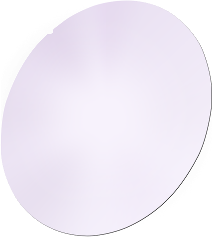
- Epitaxial Wafer
- Epitaxial Wafer is made by adding multi-nanometer thick silicon single crystal layer on top of Polished Wafer. EPI Wafer is used in non-memory chips such as Logic Devices and CMOS image sensors. Its demand is gradually increasing for next-generation wafers.
- 200mmNon-memory chip
-
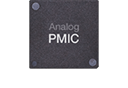 Analog (PMIC)
-
 Power Discrete
-
 CIS
CIS
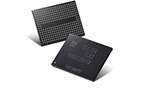
- 300mmNon-memory chip
-
 MPU
MPU
-
CIS
-
Logic (Driver IC)
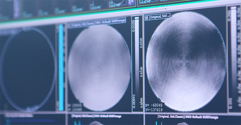
Core Technology
SK siltron offers advanced solutions for future markets that demand
higher perfection and to satisfy the various needs of
global partners based on world-class defect free crystalline,
super flat surface control and small size particles control technology.
-
- CRYSTAL DEFECT FREE
-
SK siltron designs single crystal growers using in-house technology and achieves high purity crystal quality through precision control over silicon’s
crystal defect and chemical composition.- Core Tech. 1 In-house grower design competency for high-purity crystal manufacture
- Core Tech. 2 Crystal technology for controlling contamination, defects and oxygen concentration
-
- SUPER FLAT SURFACE CONTROL
-
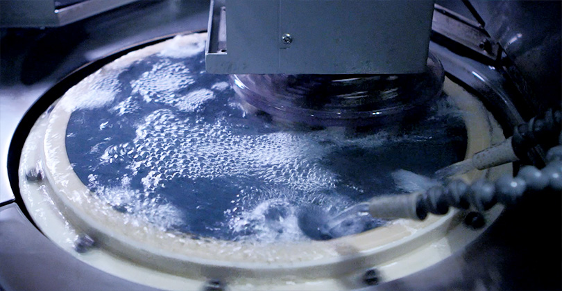
Produces zero-contamination level silicon wafers using high purity cleaning technology
- Core Tech. 1 Technology for eliminating and controlling below 1/10 billion impurity particles
- Core Tech. 2 Metal control technology within wafer surface and bulk
-
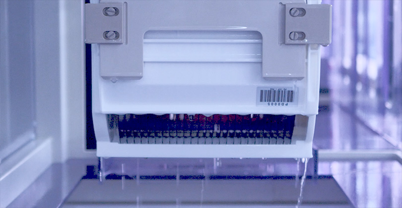
- SMALL SIZE PARTICLE CONTROL
-
Achieves optimal super flat surface through physical and chemical polishing technology.
- Core Tech. 1 Shaping control technology that improves the flatness of wafer
- Core Tech. 2 Technology for producing super flatness that eliminates deformed layers in wafers