300mm Epitaxial Wafer
Manufacturing Process
-
-
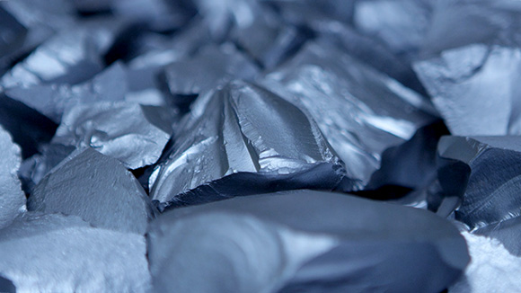
1 POLY SILICON
STACKING - Process of filling high purity poly-crystal silicon in quartz crucible
-
1 POLY SILICON
-
-
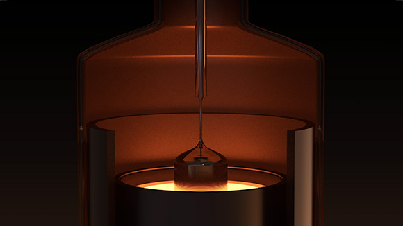
2 INGOT
GROWING - Process where poly-crystal silicon is melted in high temperature then grown into single crystal ingot
-
2 INGOT
-
-
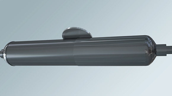
3 INGOT GRINDING
& CROPPING - Process of making the surface of ingot smooth then cropping into blocks
-
3 INGOT GRINDING
-
-
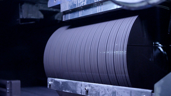
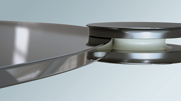
4 WIRE
SAWING - Process of cutting the ingot block into single wafers
-
4 WIRE
-
-
5 EDGE
GRINDING - Process of shaping the edge of the wafer
-
5 EDGE
-

- 6 LAPPING
- Process of making the surface of the wafer smooth and flat
-
- 7 ETCHING
- Process of eliminating process damages on wafer surface using chemical reaction
-
-
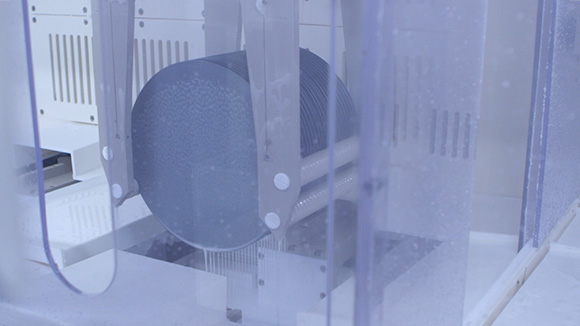
8 DOUBLE
SIDE GRINDING - Process of removing small bumps on the wafer surface
-
8 DOUBLE
-
- 9 POLISHING
- Process of removing fine bumps on the wafer through precision processing
-
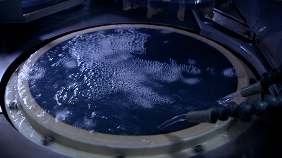
- 10 CLEANING
- Process of eliminating impurities on the wafer surface
-

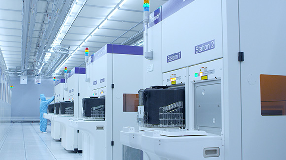
- 11 INSPECTION
- Process of inspecting the quality of wafer such as shape and flatness
-
-
12 PARTICLE
COUNTING - Process of inspecting defects in wafer surface
-
12 PARTICLE
-

-
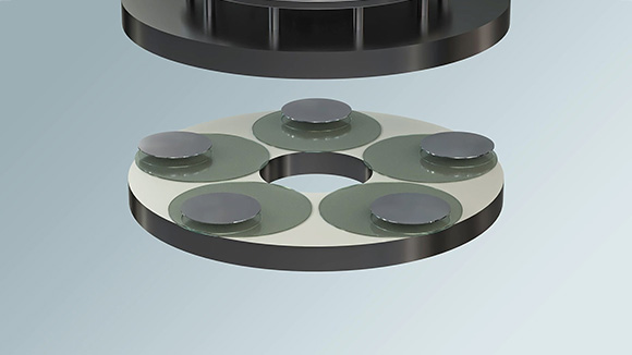
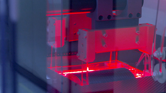
13 EPITAXIAL
GROWING - Process of adding silicon single crystal layer on wafers
-
13 EPITAXIAL
-
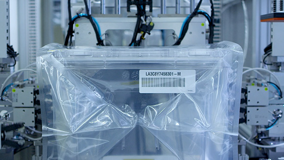
- 14 PACKING
- Process of packaging the product to protect it from shock, dust and humidity